Tungsten Copper Electronic Packaging Substrate
1. What's Tungsten Copper Electronic Packaging Substrate?
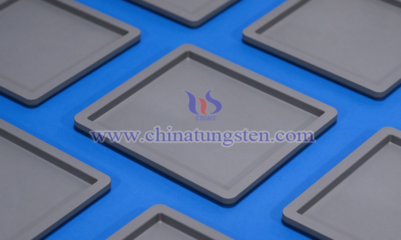
Tungsten copper electronic packaging substrate is tungsten-copper composite substrate used for electronic device packaging. It can serve as packaging base plate, heat sink, or heat-spreading component for power semiconductors, radio-frequency devices, and optoelectronic devices, simultaneously providing chip support, heat conduction, and thermal-expansion matching. CTIA's tungsten copper electronic packaging substrate is usually prepared by infiltration method: tungsten powder is first pressed and sintered into porous tungsten skeleton, after which molten copper is infiltrated into the pores to form dense composite material.
2. Characteristics of CTIA's Tungsten Copper Electronic Packaging Substrate
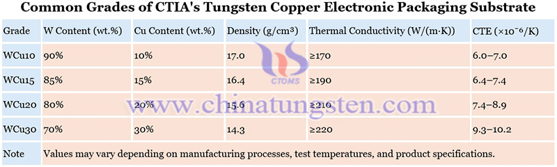
(1) Adjustable Coefficient of Thermal Expansion: Coefficient of thermal expansion varies with tungsten-copper ratio. Reference range of common tungsten copper materials is approximately 6×10⁻⁶ to 10×10⁻⁶/K, helping reduce thermal stress between chip and packaging material.
(2) Good Thermal Conductivity: Thermal conductivity may reach approximately 170–260 W/(m·K) depending on material ratio and manufacturing process, balancing chip heat dissipation with thermal-expansion matching.
(3) High Strength: Tungsten skeleton possesses high rigidity and strength, suitable for packaging structures that require flatness, dimensional accuracy, and reliability under temperature cycling.
(4) Good Densification: High density helps form continuous heat-conduction paths and meets material requirements of hermetic packages. Final hermeticity still depends on substrate structure, joining process, and inspection results.
(5) Performance Designable on Demand: High-tungsten-content materials usually offer lower coefficient of thermal expansion; high-copper-content materials usually offer higher thermal conductivity and electrical conductivity.
3. Common Grades of CTIA's Tungsten Copper Electronic Packaging Substrate
Common grades of CTIA's tungsten copper electronic packaging substrates are shown in the picture below:
4. Applications of CTIA's Tungsten Copper Electronic Packaging Substrate
(1) Power Semiconductor Packaging: Used as package baseplates and heat sinks for Gallium Nitride (GaN), Silicon Carbide (SiC) power devices, and Insulated-Gate Bipolar Transistor (IGBT) modules, balancing heat dissipation and CTE matching.
(2) RF and Microwave Devices: Used in Radio Frequency (RF) power amplifiers for Fifth-Generation (5G) base stations, millimeter-wave components, and radar RF modules, meeting heat dissipation and dimensional stability requirements of high-power-density devices.
(3) Laser and Optical Communication Devices: Used as heat sinks and submounts for laser diodes, pump lasers, and optical communication modules, helping dissipate heat quickly and reduce CTE mismatch between chips and packaging materials.
(4) New Energy Vehicle Power Modules: Used in thermal management components for electric vehicle traction inverters, onboard power electronics, and charging modules, accommodating high thermal loads and thermal cycling conditions.
(5) High-Reliability Electronic Packaging: Used as packaging substrates and heat sinks for airborne and spaceborne aerospace electronics and high-reliability microwave components, meeting heat dissipation, structural stability, and packaging reliability requirements under demanding operating conditions.
5. Specifications of CTIA's Tungsten Copper Electronic Packaging Substrate
(1) Common Material: WCu10, WCu15, WCu20, WCu30, etc.
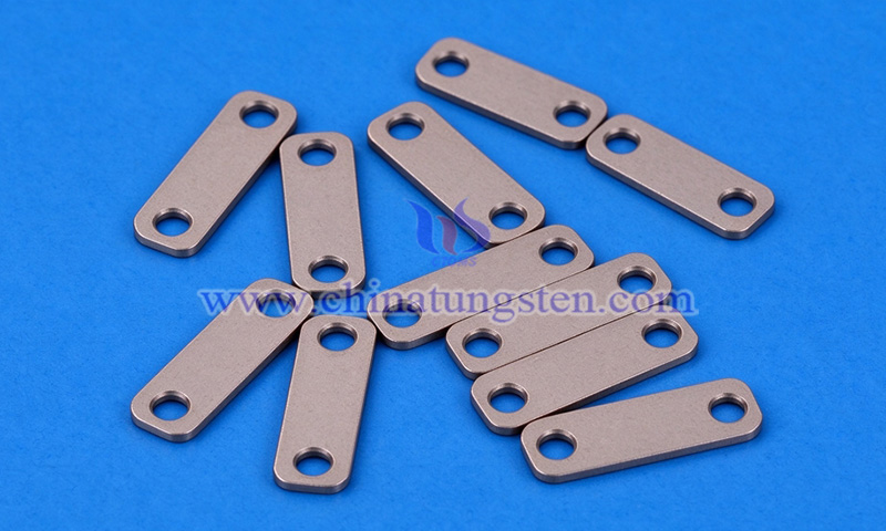
(2) Shape: Square, rectangular, and custom geometries.
(3) Dimension: Length, width, and thickness customizable according to requirements.
(4) Machining Accuracy: Dimensional tolerances, flatness, parallelism, and surface roughness customizable.
(5) Surface Finishes: Nickel plating, gold plating, etc.
CTIA GROUP has nearly 30 years of experience in tungsten copper alloy manufacturing, with extensive expertise in powder metallurgy and precision machining. CTIA provides material selection, structural design, dimensional customization, and precision machining solutions for tungsten copper electronic packaging substrates according to chip materials, packaging structures, thermal conductivity, and CTE matching requirements.
For any inquiry, please contact tungsten copper manufacturer: CTIA GROUP
Email: sales@chinatungsten.com
Tel: 0086 592 5129696 / 0086 592 5129595
Website: tungsten-copper.com
WeChat: